- 您现在的位置:买卖IC网 > Sheet目录487 > NTD24N06LG (ON Semiconductor)MOSFET N-CH 60V 24A DPAK
�� �
�
�NTD24N06L,� STD24N06L�
�6�
�5�
�Q� T�
�1000�
�4�
�Q� 1�
�Q� 2�
�V� GS�
�100�
�t� r�
�3�
�t� f�
�t� d(off)�
�2�
�10�
�t� d(on)�
�1�
�0�
�0�
�4� 8�
�12�
�I� D� =� 24� A�
�T� J� =� 25� °� C�
�16�
�20�
�1�
�1�
�10�
�V� DS� =� 30� V�
�I� D� =� 24� A�
�V� GS� =� 5� V�
�100�
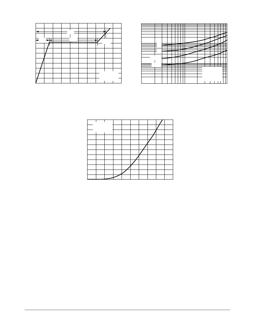
�Q� G� ,� TOTAL� GATE� CHARGE� (nC)�
�Figure� 8.� Gate� ?� To� ?� Source� and� Drain� ?� To� ?� Source�
�Voltage� versus� Total� Charge�
�R� G� ,� GATE� RESISTANCE� (OHMS)�
�Figure� 9.� Resistive� Switching� Time�
�Variation� versus� Gate� Resistance�
�DRAIN� ?� TO� ?� SOURCE� DIODE� CHARACTERISTICS�
�24�
�20�
�16�
�12�
�8�
�4�
�V� GS� =� 0� V�
�T� J� =� 25� °� C�
�0�
�0.6�
�0.68� 0.76�
�0.84� 0.92�
�1�
�V� SD� ,� SOURCE� ?� TO� ?� DRAIN� VOLTAGE� (VOLTS)�
�Figure� 10.� Diode� Forward� Voltage� versus� Current�
�SAFE� OPERATING� AREA�
�The� Forward� Biased� Safe� Operating� Area� curves� define�
�the� maximum� simultaneous� drain� ?� to� ?� source� voltage� and�
�drain� current� that� a� transistor� can� handle� safely� when� it� is�
�forward� biased.� Curves� are� based� upon� maximum� peak�
�junction� temperature� and� a� case� temperature� (T� C� )� of� 25� °� C.�
�Peak� repetitive� pulsed� power� limits� are� determined� by� using�
�the� thermal� response� data� in� conjunction� with� the� procedures�
�discussed� in� AN569,� “Transient� Thermal� Resistance� ?�
�General� Data� and� Its� Use.”�
�Switching� between� the� off� ?� state� and� the� on� ?� state� may�
�traverse� any� load� line� provided� neither� rated� peak� current�
�(I� DM� )� nor� rated� voltage� (V� DSS� )� is� exceeded� and� the�
�transition� time� (t� r� ,t� f� )� do� not� exceed� 10� m� s.� In� addition� the� total�
�power� averaged� over� a� complete� switching� cycle� must� not�
�exceed� (T� J(MAX)� ?� T� C� )/(R� q� JC� ).�
�A� Power� MOSFET� designated� E� ?� FET� can� be� safely� used�
�reliable� operation,� the� stored� energy� from� circuit� inductance�
�dissipated� in� the� transistor� while� in� avalanche� must� be� less�
�than� the� rated� limit� and� adjusted� for� operating� conditions�
�differing� from� those� specified.� Although� industry� practice� is�
�to� rate� in� terms� of� energy,� avalanche� energy� capability� is� not�
�a� constant.� The� energy� rating� decreases� non� ?� linearly� with� an�
�increase� of� peak� current� in� avalanche� and� peak� junction�
�temperature.�
�Although� many� E� ?� FETs� can� withstand� the� stress� of�
�drain� ?� to� ?� source� avalanche� at� currents� up� to� rated� pulsed�
�current� (I� DM� ),� the� energy� rating� is� specified� at� rated�
�continuous� current� (I� D� ),� in� accordance� with� industry� custom.�
�The� energy� rating� must� be� derated� for� temperature� as� shown�
�in� the� accompanying� graph� (Figure� 12).� Maximum� energy� at�
�currents� below� rated� continuous� I� D� can� safely� be� assumed� to�
�equal� the� values� indicated.�
�in� switching� circuits� with� unclamped� inductive� loads.� For�
�http://onsemi.com�
�5�
�发布紧急采购,3分钟左右您将得到回复。
相关PDF资料
NTD25P03L1G
MOSFET P-CH 30V 25A IPAK3
NTD2955PT4G
MOSFET P-CH 60V 12A DPAK
NTD3055-094G
MOSFET N-CH 60V 12A DPAK
NTD3055-150T4
MOSFET N-CH 60V 9A DPAK
NTD3055L104
MOSFET N-CH 60V 12A DPAK
NTD3055L170-001
MOSFET N-CH 60V 9A IPAK
NTD30N02T4
MOSFET N-CH 24V 30A DPAK
NTD32N06LT4G
MOSFET N-CH 60V 32A DPAK
相关代理商/技术参数
NTD24N06LT4
功能描述:MOSFET 24V 60A N-Channel RoHS:否 制造商:STMicroelectronics 晶体管极性:N-Channel 汲极/源极击穿电压:650 V 闸/源击穿电压:25 V 漏极连续电流:130 A 电阻汲极/源极 RDS(导通):0.014 Ohms 配置:Single 最大工作温度: 安装风格:Through Hole 封装 / 箱体:Max247 封装:Tube
NTD24N06LT4G
功能描述:MOSFET 24V 60A POWER MOSFET RoHS:否 制造商:STMicroelectronics 晶体管极性:N-Channel 汲极/源极击穿电压:650 V 闸/源击穿电压:25 V 漏极连续电流:130 A 电阻汲极/源极 RDS(导通):0.014 Ohms 配置:Single 最大工作温度: 安装风格:Through Hole 封装 / 箱体:Max247 封装:Tube
NTD24N06T4
功能描述:MOSFET 24V 60A N-Channel RoHS:否 制造商:STMicroelectronics 晶体管极性:N-Channel 汲极/源极击穿电压:650 V 闸/源击穿电压:25 V 漏极连续电流:130 A 电阻汲极/源极 RDS(导通):0.014 Ohms 配置:Single 最大工作温度: 安装风格:Through Hole 封装 / 箱体:Max247 封装:Tube
NTD24N06T4G
功能描述:MOSFET 24V 60A N-Channel RoHS:否 制造商:STMicroelectronics 晶体管极性:N-Channel 汲极/源极击穿电压:650 V 闸/源击穿电压:25 V 漏极连续电流:130 A 电阻汲极/源极 RDS(导通):0.014 Ohms 配置:Single 最大工作温度: 安装风格:Through Hole 封装 / 箱体:Max247 封装:Tube
NTD25
制造商:EDI 制造商全称:Electronic devices inc. 功能描述:HIGH VOLTAGE-HIGH CURRENT SILICON RECTIFIERS
NTD25P03
制造商:ONSEMI 制造商全称:ON Semiconductor 功能描述:Power MOSFET
NTD25P03L
功能描述:MOSFET -30V -25A P-Channel RoHS:否 制造商:STMicroelectronics 晶体管极性:N-Channel 汲极/源极击穿电压:650 V 闸/源击穿电压:25 V 漏极连续电流:130 A 电阻汲极/源极 RDS(导通):0.014 Ohms 配置:Single 最大工作温度: 安装风格:Through Hole 封装 / 箱体:Max247 封装:Tube
NTD25P03L_06
制造商:ONSEMI 制造商全称:ON Semiconductor 功能描述:Power MOSFET -25 Amp, -30 Volt